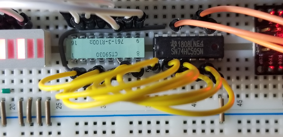
The 74HC595 is a CMOS logic device that functions as an 8-bit Serial-Input / Serial or Parallel-Output shift register with latched 3-State Outputs. The shift register accepts serial data and provides a serial output. The shift register also provides parallel data to the 8–bit latch. The shift register and latch have independent clock inputs. This device also has an asynchronous reset for the shift register. It is especially useful as it directly interfaces with the SPI serial data port on CMOS MPUs and MCUs.
This project demonstrates the typical practical use of the shift register by counting up in binary from 0 to 255. It shifts the presence of serial data from right to left and left to right as that data is clocked through the register from an Arduino Nano. The Nano provides the data, the clock, and latch control to present output data to an LED array.
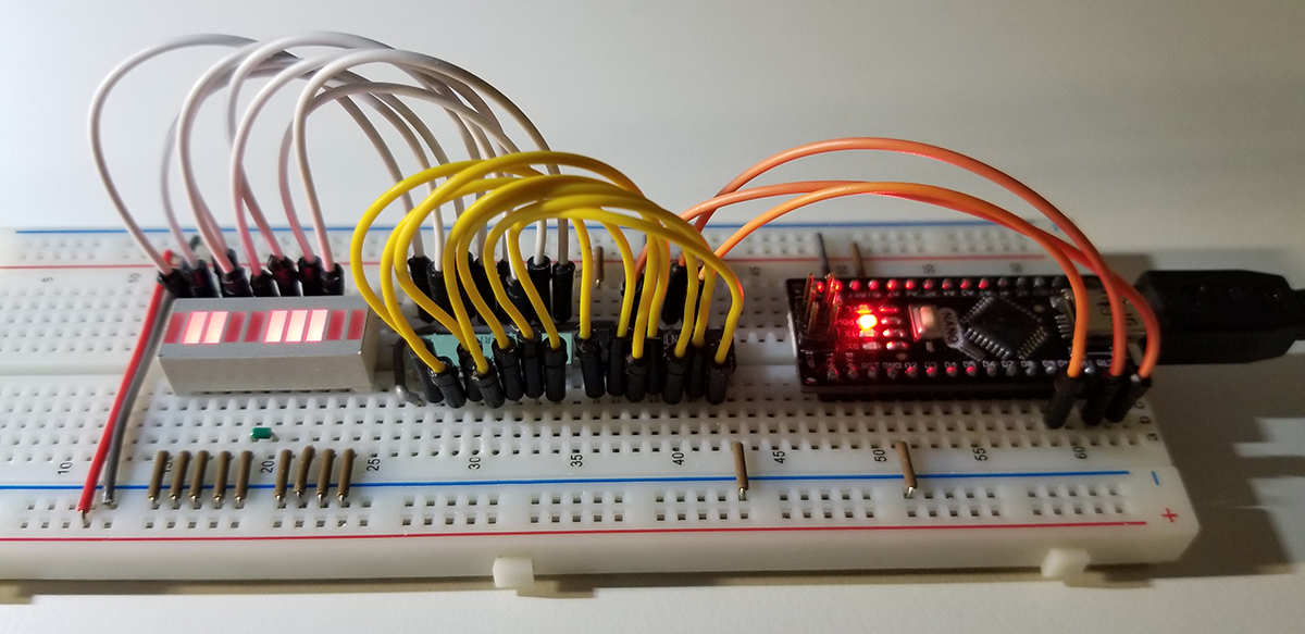
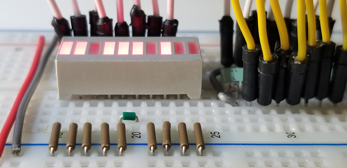
As inputs are cycled through the register, binary state changes are visually represented at the LED array. Each LED from left to right is a single bit from 0 to 7. Left most LED is the most significant bit (MSB) and the right most LED is the least significant bit (LSB). The two LEDs at the right end of the array are inactive in this project.
The datasheet of the 74HC595 provides added details concerning operating descriptions, limits, timing waveforms, testing conditions, and packaging. The purpose of the device centers around the conversion of serial input data to serial or parallel outputs through its internal shift register. Most typically, as serial data is applied to the register’s input, the data becomes transposed to parallel outputs across 8 separate pins. Outputs present at those pins are held as a latch until delivery is permitted by a control pin to deliver serial data when desired as a matter of timing or synchronization.
| Pin Descriptions |
|---|
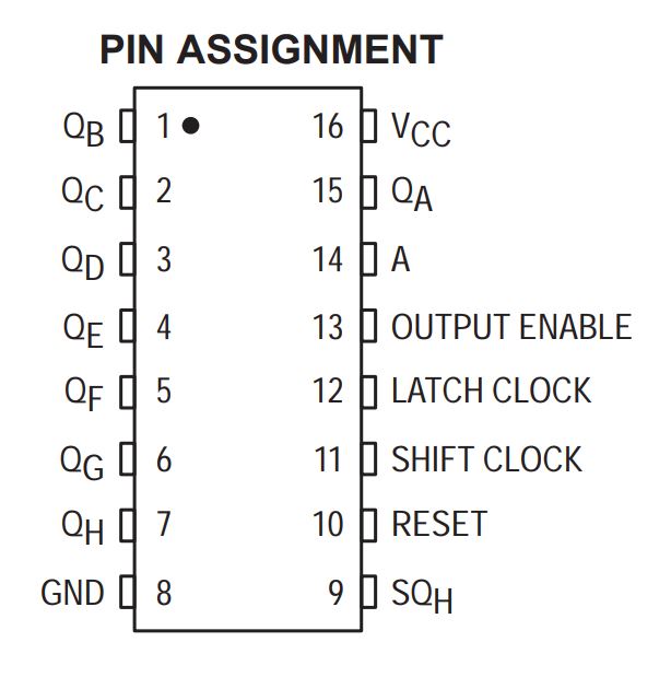
| INPUTS A (Pin 14) Serial Data Input. The data on this pin is shifted into the 8–bit serial shift register. |
| CONTROL INPUTS Shift Clock (Pin 11) Shift Register Clock Input. A low– to–high transition on this input causes the data at the |
| Reset (Pin 10) Active–low, Asynchronous, Shift Register Reset Input. A low on this pin resets the shift register portion of this device only. The 8–bit latch is not affected. |
| Latch Clock (Pin 12) Storage Latch Clock Input. A low–to–high transition on this input latches the shift register data. |
| Output Enable (Pin 13) Active–low Output Enable. A low on this input allows the data from the latches to be presented at the outputs. A high on this input forces the outputs (QA–QH) into the high–impedance state. The serial output is not affected by this control unit. |
| OUTPUTS QA – QH (Pins 15, 1, 2, 3, 4, 5, 6, 7) Noninverted, 3–state, latch outputs. |
| SQH (Pin 9) Noninverted, Serial Data Output. This is the output of the eighth stage of the 8–bit shift register. This output does not have three–state capability. |
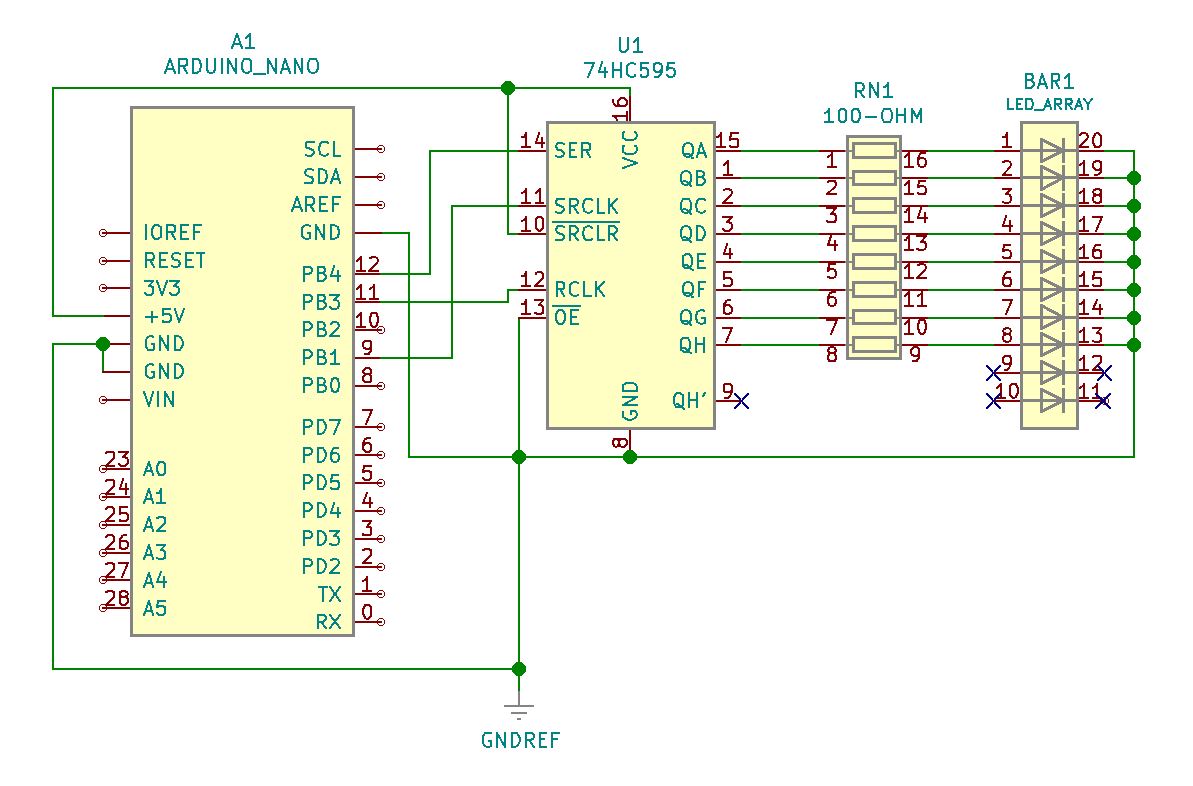
Project Schematic:
The system components consist of an Arduino Nano, a 74HC595 8-bit shift register, a 100-ohm resistor pack, and an LED array. Together these components are assembled to support the code necessary to deliver computer or user data to a collection of outputs (QA through QH). All 8-bits of data are shifted through the device from the Arduino (pin 9) to the shift register control (pin 11). The serial data received at pin 14 of the register becomes internally transposed and placed to outputs QA through QH as the data is latch clocked on its state transitions to the outputs via the R-clock control pin at pin 12.
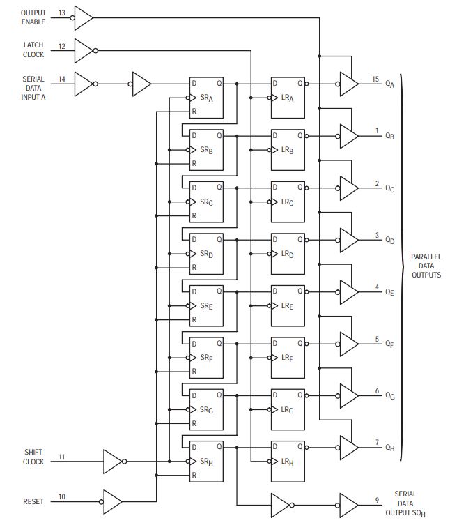
74HC595 Logic Diagram:
Data and control functions indicate the serial input to parallel output states made possible through grouped flip-flops. State propagation is triggered among all flip flops through latch clock edge transitions as illustrated at each flip flop in the diagram.
Project Review:
Code Example:
int latchPin=11;
int clockPin=9;
int dataPin=12;
int dt=100;
byte Bytes=0b11111110; //circular shift left with 1 LED Off
//byte Bytes=0b00000001; //circular shift left with 1 LED On
void setup()
{
Serial.begin(9600);
pinMode(latchPin,OUTPUT);
pinMode(dataPin,OUTPUT);
pinMode(clockPin,OUTPUT);
}
void loop()
{
digitalWrite(latchPin,LOW);
shiftOut(dataPin,clockPin,LSBFIRST,Bytes);
digitalWrite(latchPin,HIGH);
delay(dt);
Serial.println(Bytes);
Bytes=Bytes/128+Bytes2; // circular shift left
//Bytes=Bytes128+Bytes/2; // circular shift right
}


Comments are closed.