Archive | Projects RSS feed for this section

USB-C Male Breakout Module

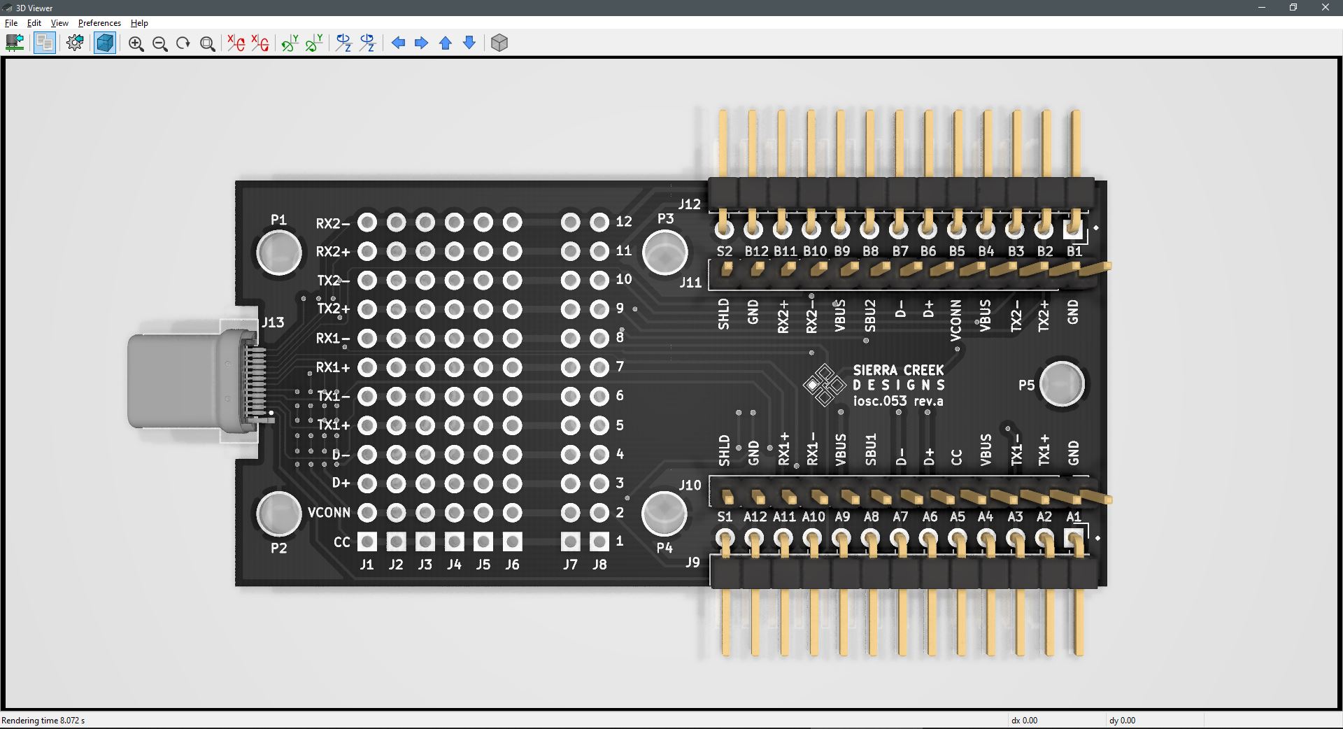
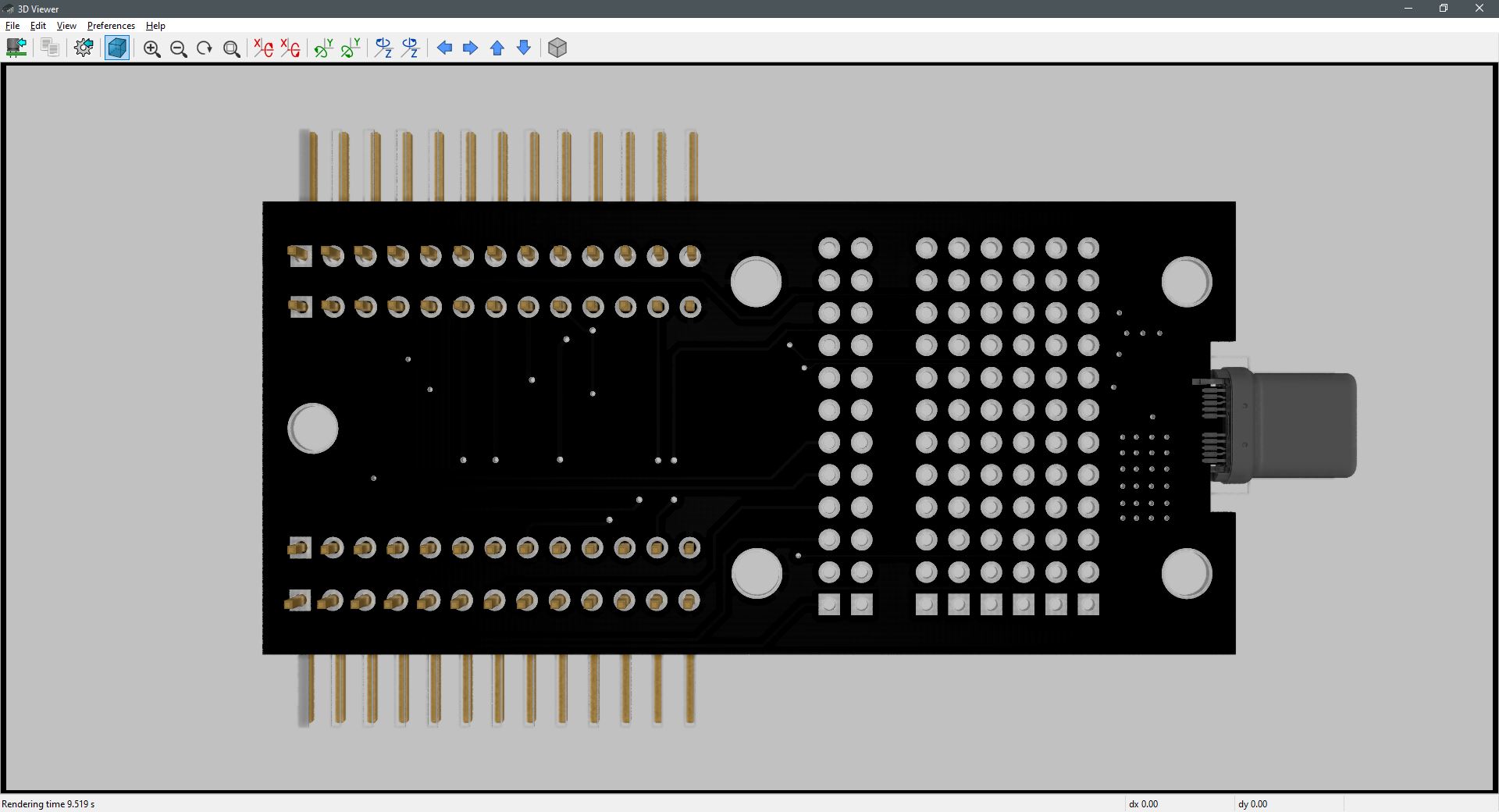
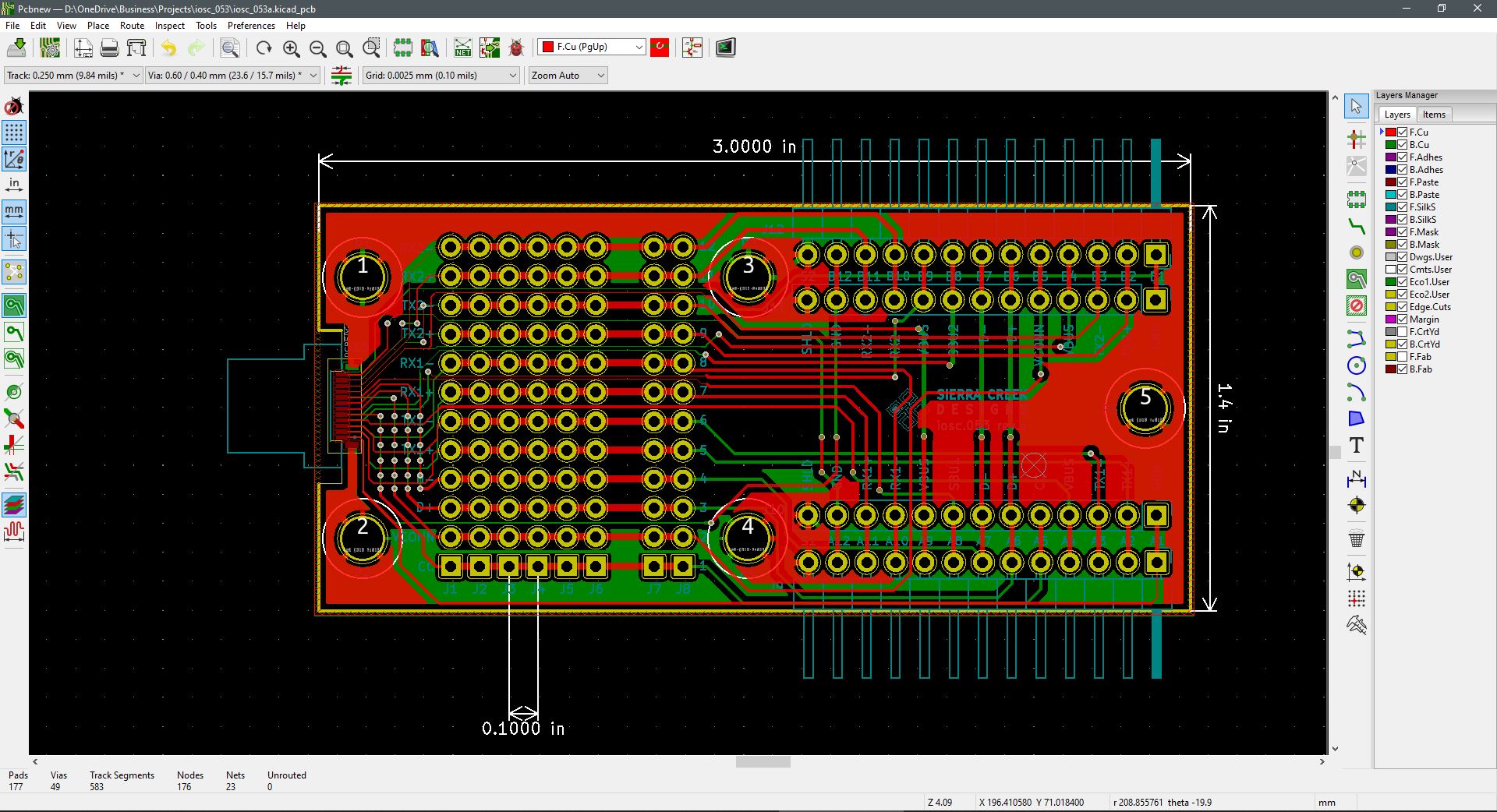
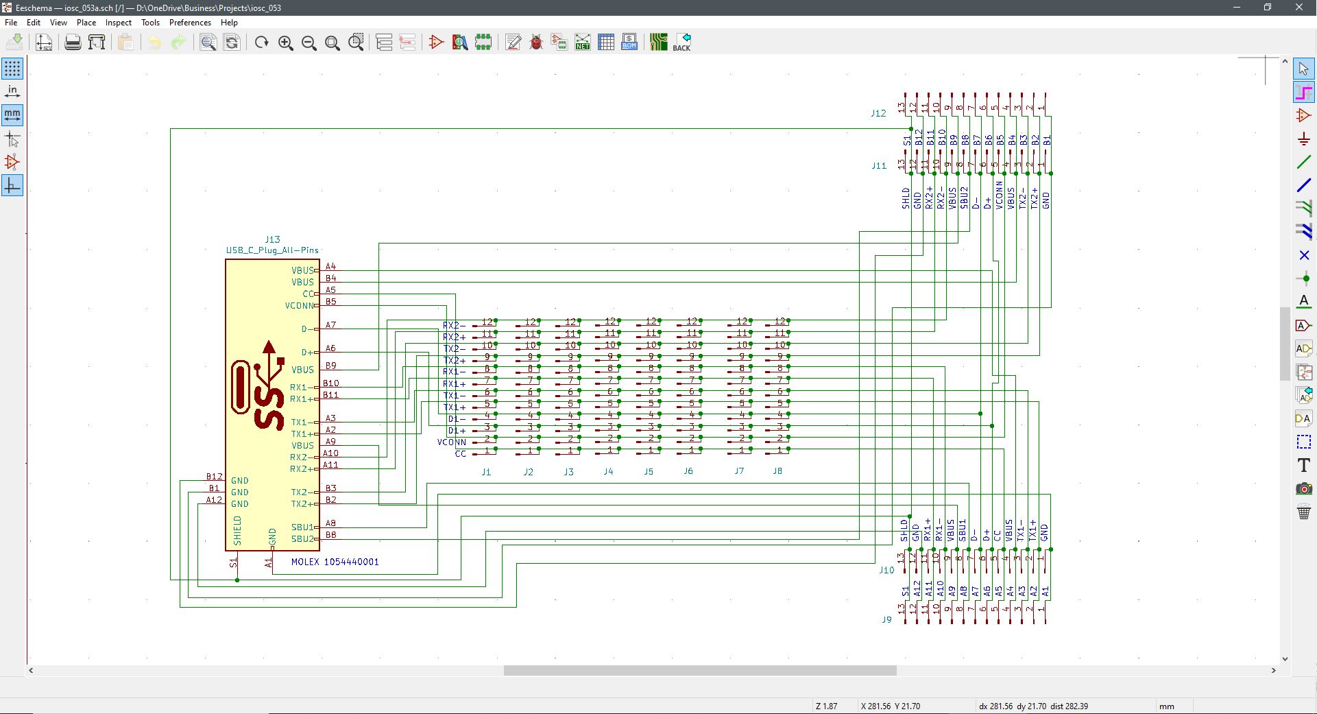
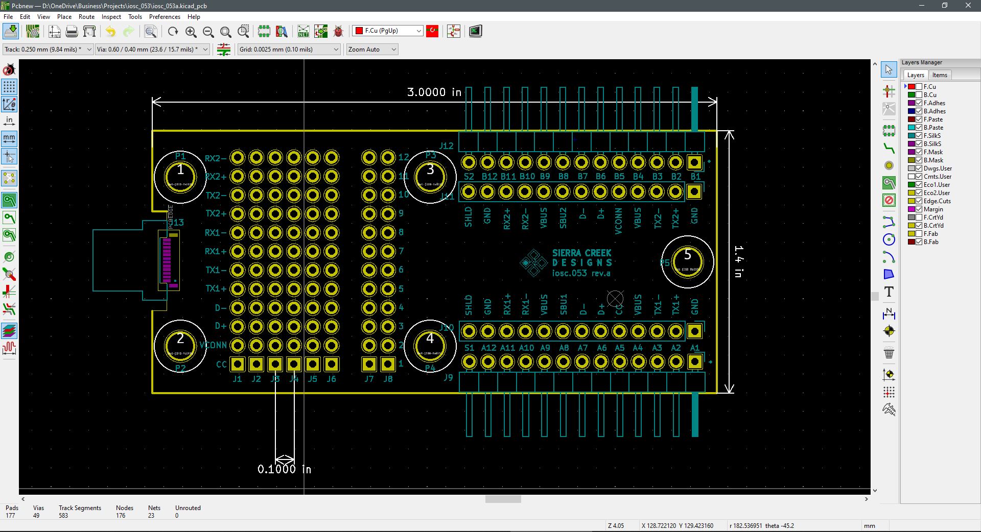
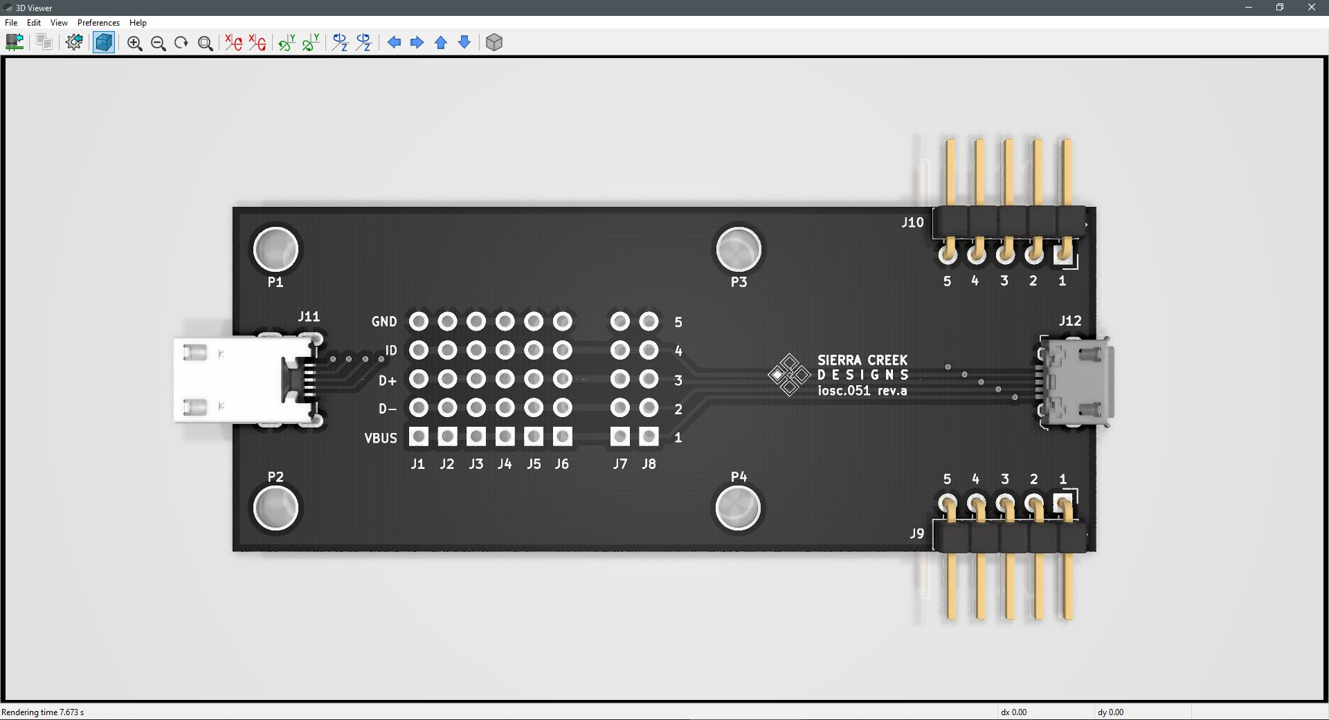
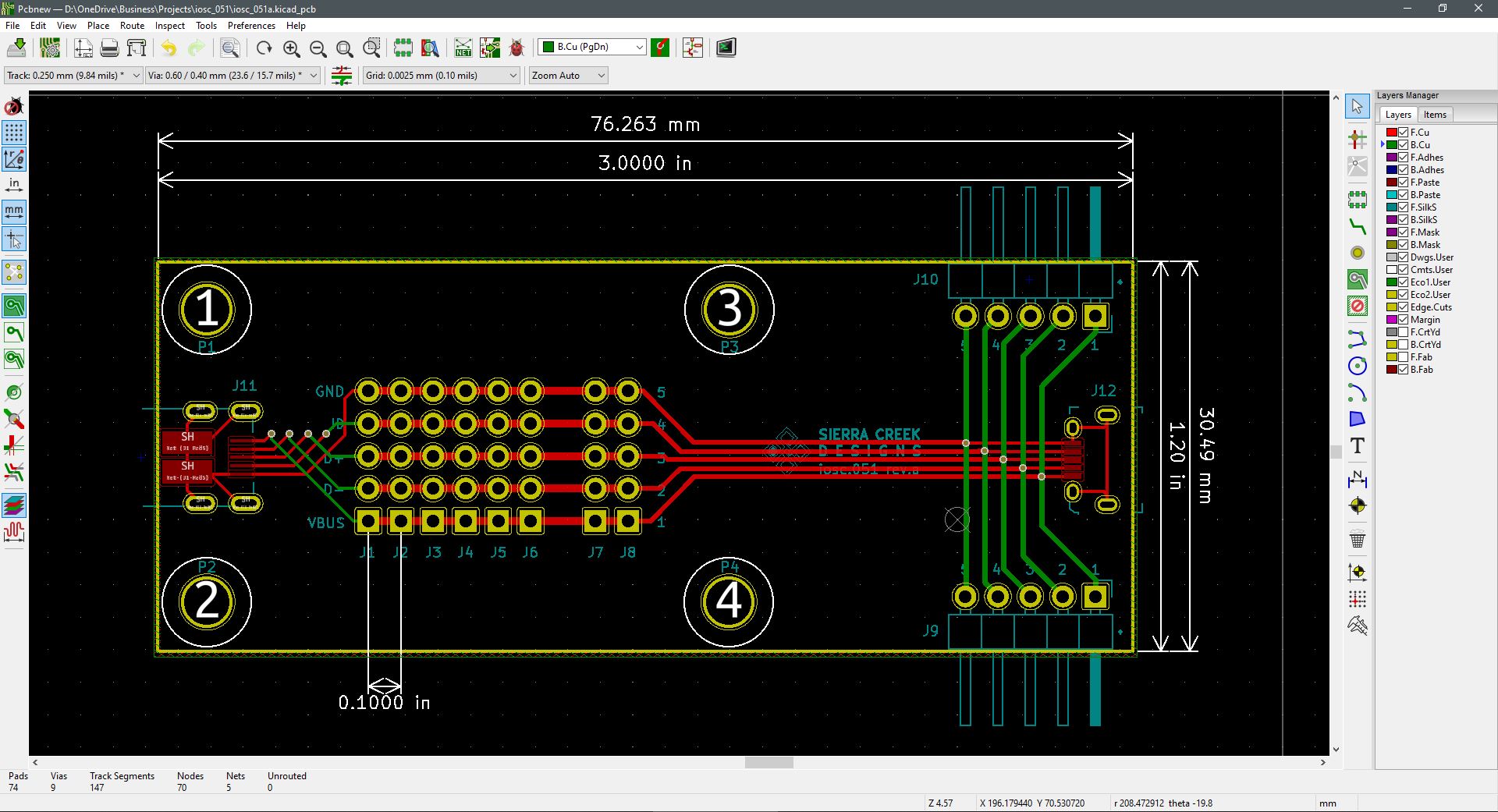
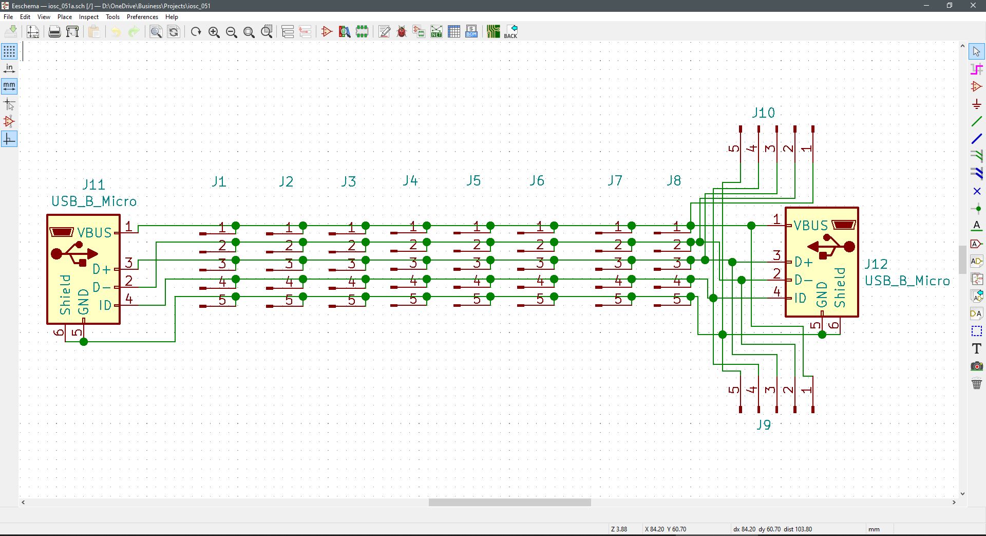
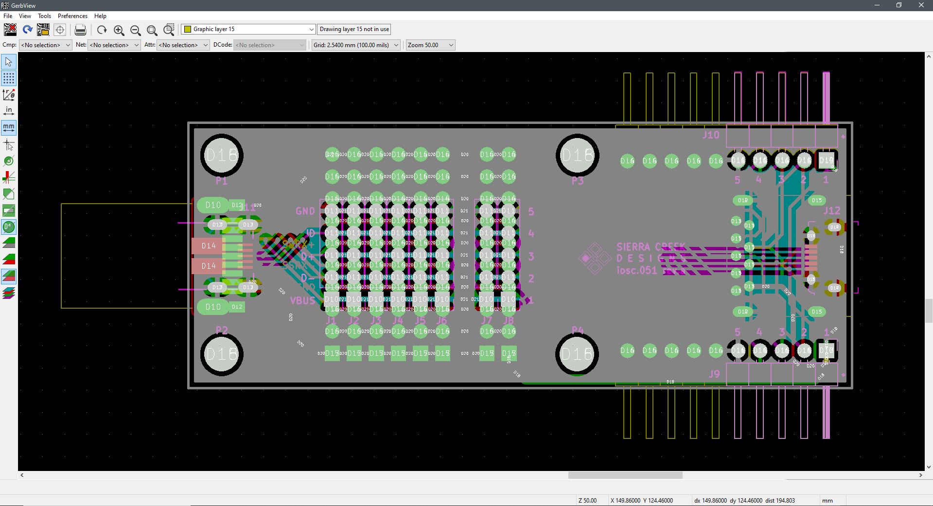
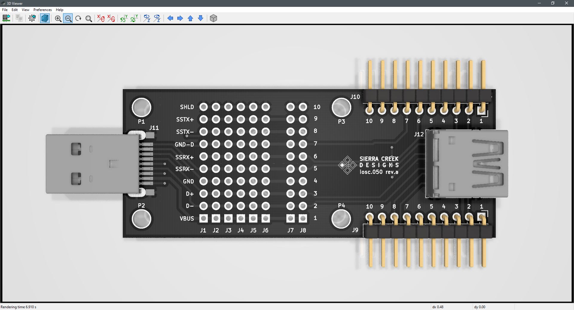
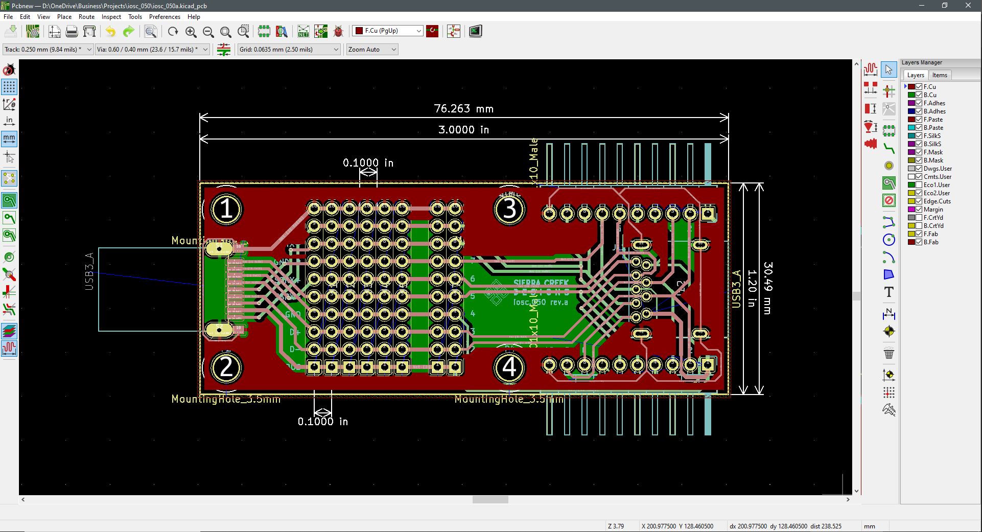
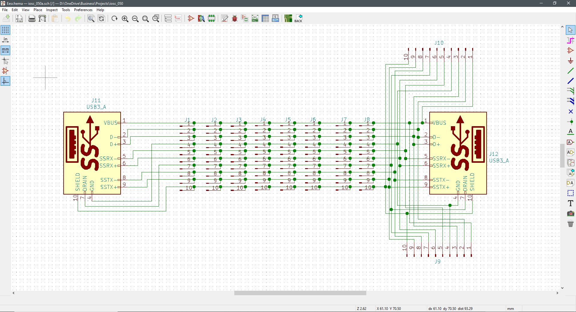
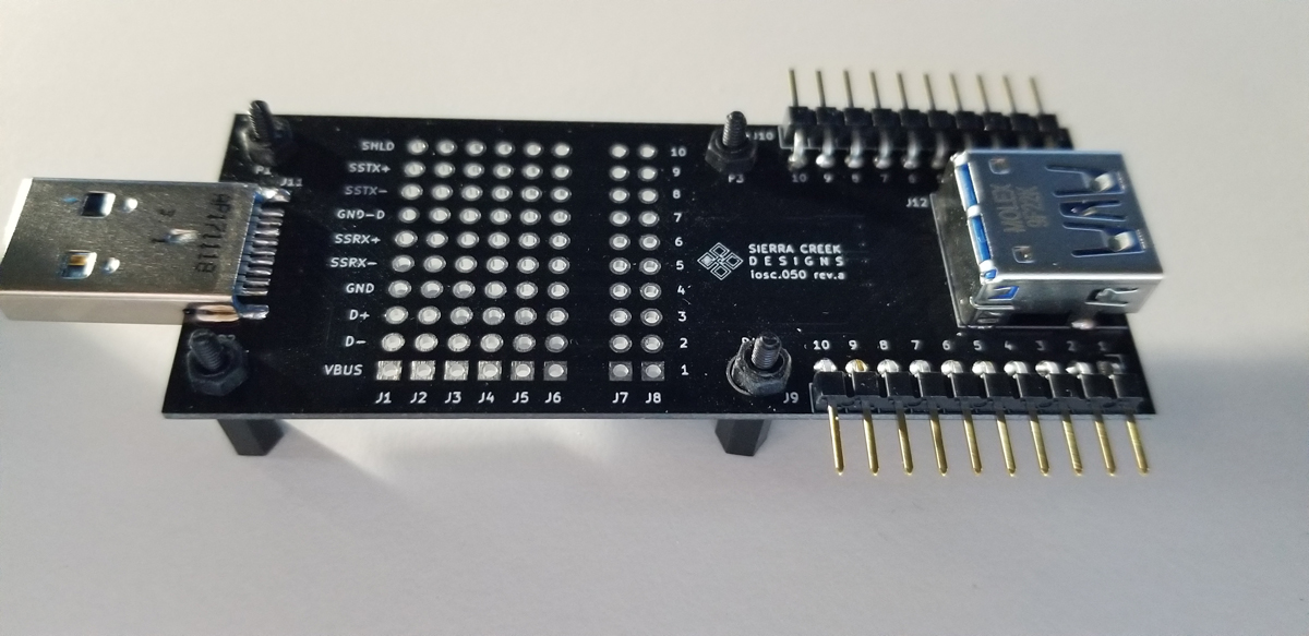
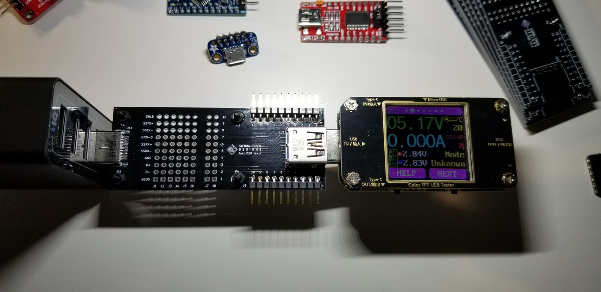
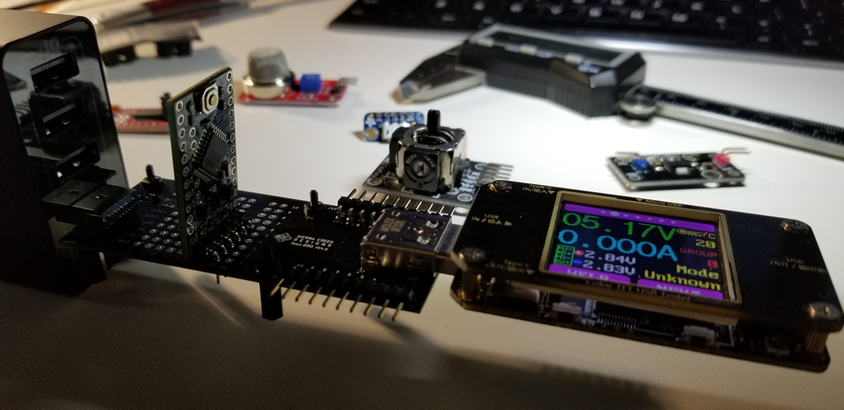
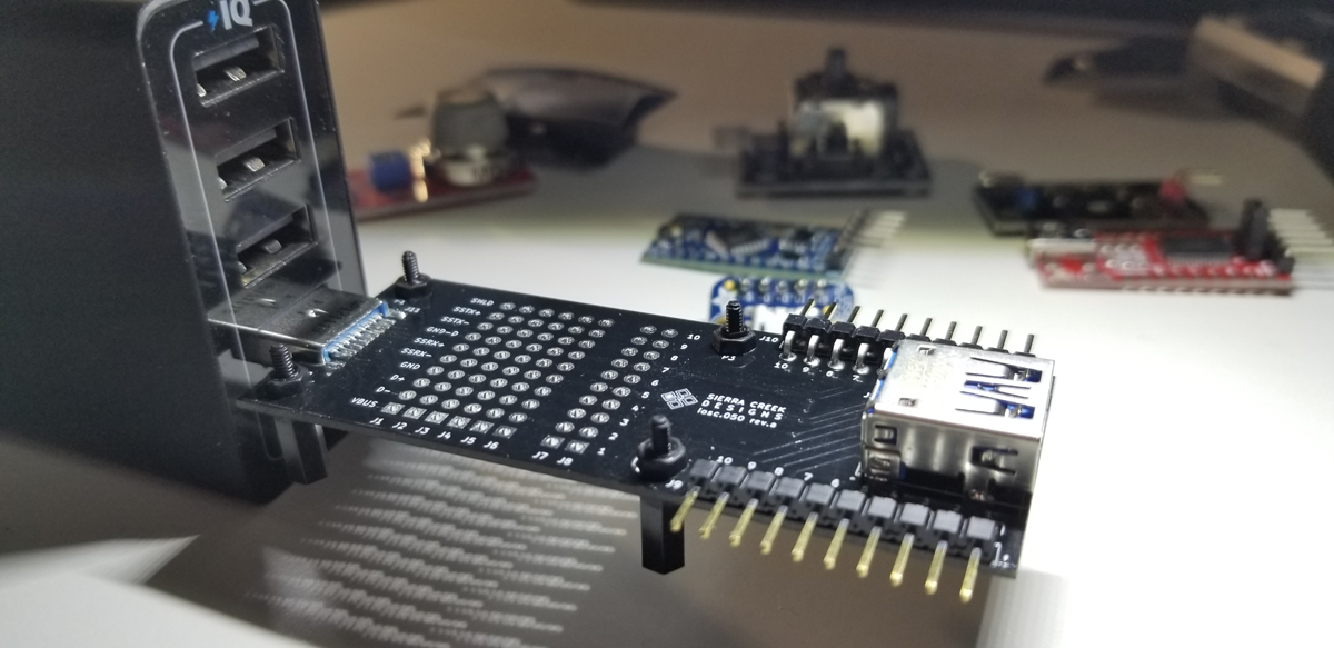
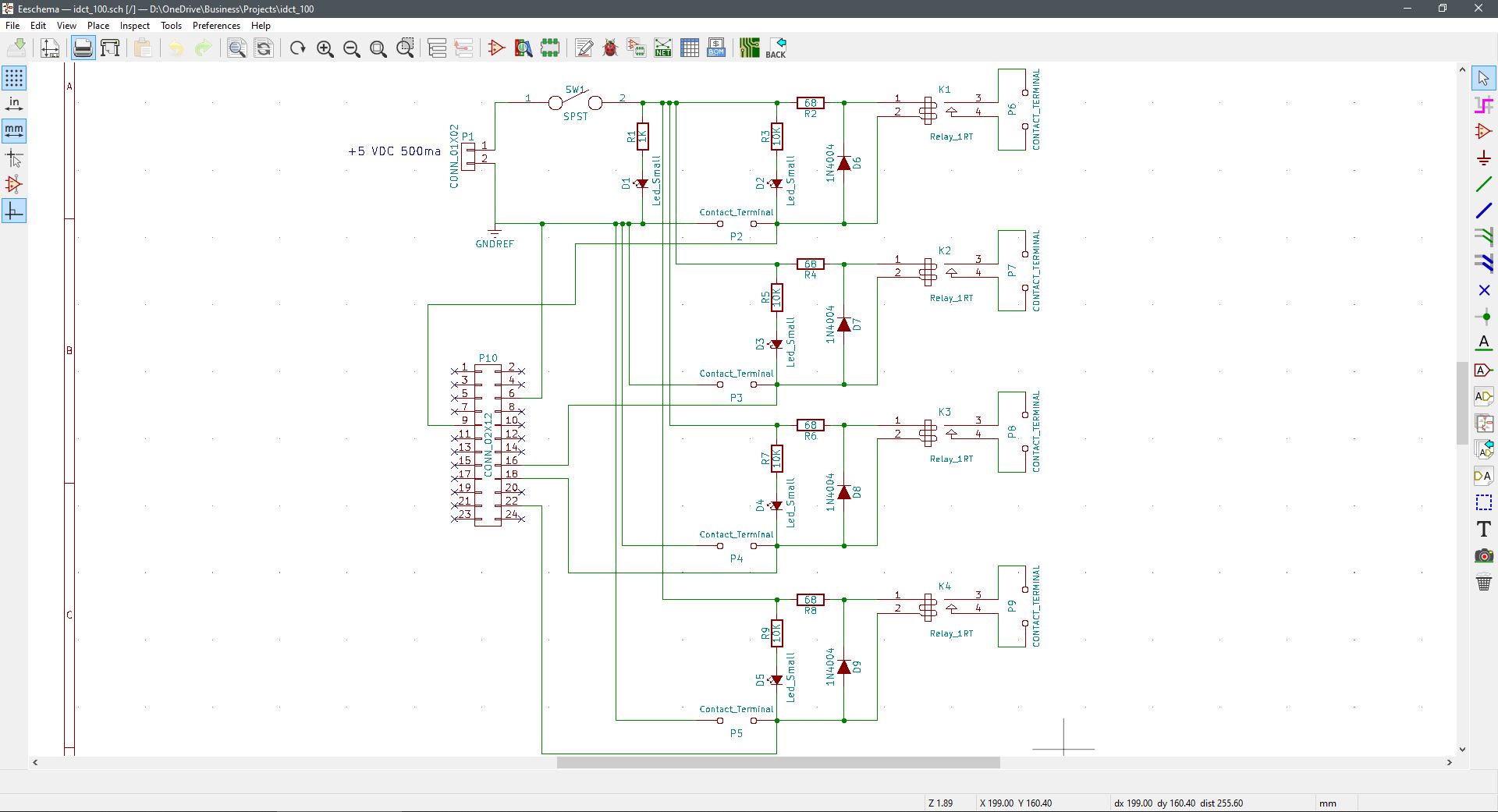
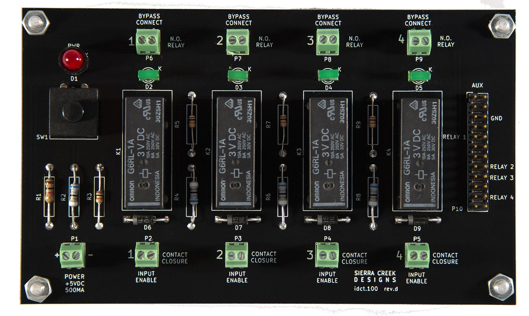
This USB-C breakout module is designed to separate out all pins and the shield of a standard 24-pin USB-C plug connector. As with prior USB breakout modules, each pin is grouped together on a grid for ease of measurement of signal levels and communication. Data and control lines are presented at connectors J1- J8 without VBUS or ground connections. The VBUS, ground, and shield connections are available at the pin-headers J9 – J12. The mounting holes P1 – P5 are connected to the entire shield path among all connections.

Connectors J9 and J10 are in parallel as physical connections to each other. Just the same as J11 and J12. These paired pin-headers are set up this way to support either ribbon cable terminations or perforated board placement while leaving open the pin connections for additional breakout aside from the grid between J1 and J8.

USB-Micro Breakout Module

The primary difference with this USB-B Micro breakout module and the earlier developed model is the USB-A receptacle at its output. The J11 input to J12 output is a straight-through except for the Micro-USB path to J8. This connection is severed to assure an output from a connected device doesn’t become unnecessarily grounded. The other side of J8 is connected to both ground and shield to assure pin-4 is grounded as per the USB-A connection standard.

If it is desired or necessary to ground the ID pin along the later connectors J1 through J8, then use a jumper/shunt block. This connection has a standard 0.1″ pin separation.

As described earlier, this module only provides for 5-pins including shield terminations. Specifically, pinout connections corresponding to USB 2.0. The input plug extends to the output receptacle with numerous signal and voltage tap points in-between.

Then as before with the USB-micro break out module, these through-hole connections serve as a grid of tap points for purposes of measurement, or to add an external device for peripheral functions (J1 – J8). The female receptacle is the input at J11 and the other female receptacle is at the output at J12. The 5-pin headers at J9 and J10 are simply in parallel with both the USB plug and receptacle for extended use without the need for solder work at the J1 – J8 header grid. Assuming these pads are mounted with pin-headers.


USB-B Breakout Module

This USB Micro-B breakout module is sort of a little brother of the USB-A 10-pin breakout module designs and developed earlier. This module only provides for 5-pins including shield terminations. Specifically, pinout connections corresponding to USB 2.0. The input plug extends to the output receptacle with numerous signal and voltage tap points in-between.

As before with the USB-A break out module, these through-hole connections serve as a grid of tap points for purposes of measurement, or to add an external device for peripheral functions (J1 – J8). The female receptacle is the input at J11 and the other female receptacle is the output at J12. The 5-pin headers at J9 and J10 are simply in parallel with both the USB plug and receptacle for extended use without the need for solder work at the J1 – J8 header grid.

USB-A Breakout Module

Setting up this breakout module for connectivity between a USB receptacle and a USB plug required careful attention to detail. It was necessary to pay attention to numerous factors concerning layout, component positioning, dimensioning, and port orientation. The selection of both USB connectors was somewhat tentative because of a concern for anchoring to the PCB where there is sufficient strain relief from angular forces applied to each end. Ultimately, both USB connectors chosen were through-hole to assure a secure enough physical connection. The two 0.1″ pin headers on each end correlate to the 10-pin USB3.0/3.1 pin assignments by name and number.

While the array of pads (J1 – J8) is in place to tap off signal, power, and ground points along the USB path, the two pin headers are hardwired in to support an electronic breadboard or perforated board mount for convenient solderability. The pin headers J9 and J10 support a vertical mount arrangement, or horizontal, depending upon the project or use-case.

Between the USB connectors, it was necessary to route the data and high-speed traces at roughly equal length distribution and copper thickness. This helps to assure there are no unnecessary voltage level losses and unwanted heat stresses. While this module doesn’t support the data rate specification associated with the SuperSpeed standard, it does support up to 1.0A DC of current from the USB connector power pins (USB 3.0 SuperSpeed at 5Gbit/s; also known as USB 3.1 Gen 1 SuperSpeed at 5Gbit/s; USB 3.1 Gen 2 is SuperSpeed+ with a transfer rate of 10Gbit/s). USB 3.0 SuperSpeed at 5Gbit/s; also known as USB 3.1 Gen 1 SuperSpeed at 5Gbit/s; USB 3.1 Gen 2 is SuperSpeed+ with a transfer rate of 10Gbit/s. This module is connection compatible with USB 1.0 to USB 3.1, but it is not rated for SuperSpeed performance. Largely due to the cost and scope of setting up impedance matching along the data lines with multiple isolated layers of PCB fabrication.

The purpose of this module is to provide a convenient path between two USB ports for utility or experimental reasons. If a user wishes to measure or branch off the pads or pins along a USB path, the freedom is made possible with this module to do that. Either by inserting a small bed-of-nails or by attaching through-hole parts and pins as desired.

Signal Breakout – Terminal

This module is identically the same as the 2.5mm breakout module, except the output connection is a 3-position terminal block output. This is a different module to accommodate a twisted-pair wire connection. To review the 2.5mm module, here is its description to cover relevant details for this terminal block version.

This breakout module is a micro slot module that permits the interrupt and measurement, capture, and tap of a small highspeed signal. From as low as 10Hz to millions of cycles (>3MHz), a signal’s strength is monitored, cut, interrupted, or redirected. It also supports polarity reversal from input to output. The signal output is connected to either the 2.5mm barrel output receptacle or the pin header at J7.

The module also supports current measurement through the 0.2-ohm shunt resistor or voltage capture by any available test point. An input signal’s frequency, phase, polarity, current, voltage, and activity are all observable functions made present on this module. The module also provides for a power presence LED.

The bed-of-nails at J2 is loaded with jumper blocks to complete a signal path. This connector is the point of interrupt for any device to locate in-between the input and output. Remove a jumper block for device insertion. Or remove the jumper block from the ground pins at J2 to serve as a ground lift for a floating and balanced connection. This module is a sort of swiss-army-knife of breakout boards for small signal devices.


Signal Breakout – 3.5mm

This module is identically the same as the 2.5mm breakout module, except the output connection is a 3.5mm barrel receptacle. This is a different module to accommodate a standard audio connection. To review the 2.5mm module, here is its description to cover relevant details for the 3.5mm version.

This breakout module is a micro slot module that permits the interrupt and measurement, capture, and tap of a small highspeed signal. From as low as 10Hz to millions of cycles (>3MHz), a signal’s strength is monitored, cut, interrupted, or redirected. It also supports polarity reversal from input to output. The signal output is connected to either the 2.5mm barrel output receptacle or the pin header at J7.

The module also supports current measurement through the 0.2-ohm shunt resistor or voltage capture by any available test point. An input signal’s frequency, phase, polarity, current, voltage, and activity are all observable functions made present on this module. The module also provides for a power presence LED.

The bed-of-nails at J2 is loaded with jumper blocks to complete a signal path. This connector is the point of interrupt for any device to locate in-between the input and output. Remove a jumper block for device insertion. Or remove the jumper block from the ground pins at J2 to serve as a ground lift for a floating and balanced connection. This module is a sort of swiss-army-knife of breakout boards for small signal devices.

Signal Breakout – 2.5mm

The 2.5mm breakout module is a micro slot module that permits the interrupt and measurement, capture, and tap of a small highspeed signal. From as low as 10Hz to millions of cycles (>3MHz), a signal’s strength is monitored, cut, interrupted, or redirected. It also supports polarity reversal from input to output. The signal output is connected to either the 2.5mm barrel output receptacle or the pin header at J7.

The module also supports current measurement through the 0.2-ohm shunt resistor or voltage capture by any available test point. An input signal’s frequency, phase, polarity, current, voltage, and activity are all observable functions made present on this module. The module also provides for a power presence LED.

The bed-of-nails at J2 is loaded with jumper blocks to complete a signal path. This connector is the point of interrupt for any device to locate in-between the input and output. Remove a jumper block for device insertion. Or remove the jumper block from the ground pins at J2 to serve as a ground lift for a floating and balanced connection. This module is a sort of swiss-army-knife of breakout boards for small signal devices.

Contact Closure Relay Module

The newly developed micro slot module platform affords more opportunities to bring about new and useful functions. Namely, to support specific capabilities aside from the prior micro slot modules designed to help signal transfer and breakout. Left-to-right input-to-output features for both control and signal transfer or routing, but now also new processes following the same type of transfer function.

This signal relay module is designed to support a contact closure source to allow a higher current contact path at the module’s output. When a short-circuit path is made at the Enable terminals of the module’s input connector, a relay closure event is triggered at the output. This event provides for a parallel bypass path across an attached load connected to the output connector. Or a series circuit path completion is made to allow a signal or voltage to become active at the output connector.

When the relay module is supplied with 5V; a green LED illuminates to give a user continuous visual Power status. A separate blue Activity LED indicates when the relay itself is enabled by the presence of a contact closure input. As a 5V source is applied to the micro slot module, a simple wire connection from Enable to Ground triggers the relay to complete the output connection path, which in turn illuminates the power Active LED.

Features and capabilities are outlined here to summarize what functions are available.

  • Signal Bypass
  • Circuit Closure
  • Relay Status LED
  • Power Status LED
  • Terminal Block Connectivity
  • Functional Control via Pin Headers

GPIO Relay Module

This module is a version of the relay module previously developed to support a contact closure input for activation. This module is different where it doesn’t require a contact closure, or shorted-path to activate the relay output at J2. Instead, it supports a GPIO (general purpose input/output) signal for relay activation. The other connections and functions remain the same except the mode of activation at J1 just changes in support of an SBC such as an RPi, Arduino, Espressif, Nucleo, etc. The prior module is intended for external contact closure or shorted connection at the input connector J1. Using a simple twisted pair of wires, for example.

This module required both SN74LVC1G66 analog bilateral switch and a TLV73330 low voltage dropout regulator (LDO) to translate low voltage levels from GPIO signals at 1.8, 2.8, 3.0V, or 3.3V to a steady 3.3V level necessary to set up enough source strength at the relay. It is set in series with the analog SPST switch as necessary to drive the relay (i.e. deliver GPIO signal to the relay).

The other notification LEDs are present as before to indicate the ACTIVE state of the relay and power presence at the module.

Programmable Pulse Module

This module was an early project to get on my feet concerning workflow and the process of originating micro slot modules. This is a programmable timing module that delivers a digital pulse train at a selectable rate. With a trimmable duty cycle range with VR1, it permits a 5VDC clock output by way of integer multiples. By applying jumper settings at P1, the rate of the pulse stream becomes assigned and fixed until another rate is chosen.

The module uses an 8MHz precision Abracon crystal. The microswitch at SW1 provides for a one-shot pulse for triggering purposes. The modules allow for a standard mounting via the same footprint earlier originated. The module also provides for power presence LED along with a resettable protection fuse at F1.

4-Channel Fan Module

This module is a multispeed fan module controlled by low/high selection or continuous variability by a temperature sensor (thermistor) at each fan control circuit. With a thermistor attached to an external device, one or more fans will increase or decrease their speed for changing air pressure and cooling. Each fan has a separate thermistor/temperature sensor for maximum flexibility. Conversely, all fans can be enabled at high speed to their maximum with SW1, SW2, SW3, and SW4.

The 3″ x 5″ form factor is mountable for stacking onto other modules of these dimensions. Depending upon how the fans are mounted, hot or cool air can become either injected or ejected depending upon the intended application. This module is a straight forward thermal management device that suitably accompanies single board computers or other devices that require additional derating to be improved or required longevity.

4-Channel Relay Module

In an effort to combine multiple relays onto a single module, this project accepts a single power supply (PSU). The PSU attached at the P1 terminal block provides power to all relays and associated LED indicators. The LEDs are in place to indicate the active or inactive state of each separate relay. All relays and indicators are aligned in parallel for ease of visual recognition and separation.

All changes have their dedicated input and output terminal blocks. To give an intuitive sense of what hook up terminations are necessary to operate the module. The inputs are labeled as Contact Closure to indicate a functional purpose of each connection. By applying a physical wire connection between each pin at P2, P3, P4, and P5, each relay becomes activated whereby connectors P6, P7, P8, and P9 close. As the pins at these output connectors become closed as a bypass, or completed path. All relays are normally open type components.

The terminal block is another connection point in parallel with contact closure connectors 1 – 4. Only this connector is a pin-header to support an external computer-controlled activation mechanism.